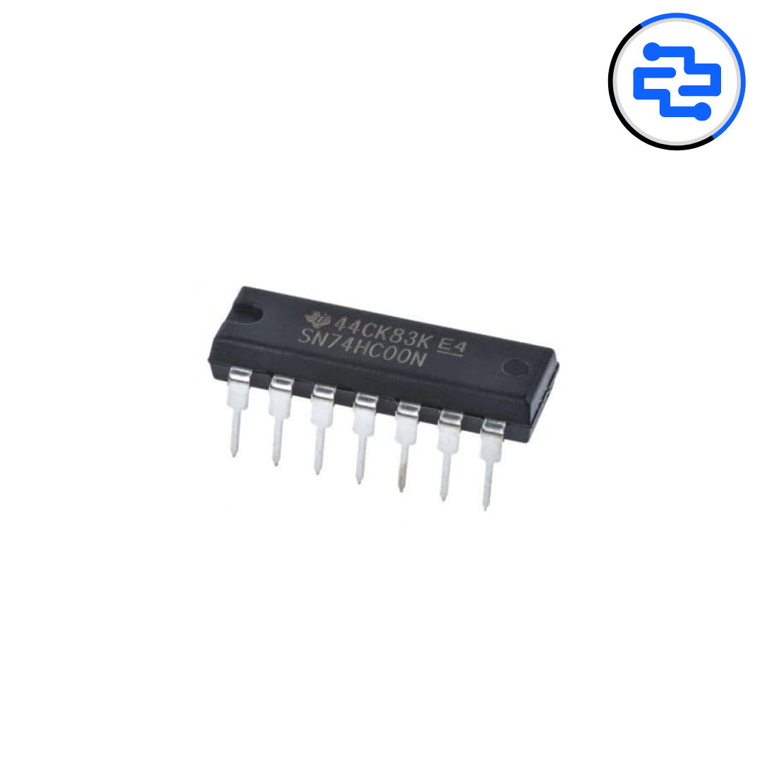
The 74HC00 is a high-speed CMOS integrated circuit containing four independent 2-input NAND gates. It operates within a wide voltage range of 2.0V to 6.0V, combining the low power consumption of CMOS technology with speeds comparable to older Low-power Schottky TTL (LSTTL) families. As a cornerstone of digital logic design, it serves as a universal building block for complex computational and signal-processing circuits.
Understanding the 74HC00 Architecture
The 74HC00 belongs to the "7400" series of integrated circuits, which has been an industry standard for decades. Specifically, the "HC" designation stands for High-speed CMOS. In the landscape of 2026, while many functions are integrated into System-on-Chip (SoC) designs or FPGAs, the 74HC00 remains indispensable for glue logic, signal buffering, and simple control systems due to its reliability and ease of implementation.
At its core, the device utilizes silicon-gate CMOS technology. This fabrication method allows for a high degree of noise immunity and very low static power consumption. Inside the 14-pin package, there are four identical, independent circuits. Each circuit performs the NAND (Not-AND) logical operation. The NAND gate is significant because it is a "universal gate," meaning any other Boolean logic function—such as AND, OR, NOT, or XOR—can be constructed using only NAND gates.
The internal structure consists of P-channel and N-channel enhancement-mode MOSFETs arranged in a complementary configuration. When both inputs are at a high logic level, the N-channel network conducts to ground, while the P-channel network is cut off, resulting in a low output. In any other input combination, the P-channel network conducts to the supply voltage ($V_{CC}$), ensuring the output remains high.
Pinout and Logical Configuration
Standardization is a hallmark of the 74-series, and the 74HC00 follows the classic 14-pin layout. Understanding this layout is the first step for any PCB designer or hobbyist working with breadboards.
Pin Assignment Table
| Pin Number | Function | Description |
|---|---|---|
| 1 | 1A | Input 1 of Gate 1 |
| 2 | 1B | Input 2 of Gate 1 |
| 3 | 1Y | Output of Gate 1 |
| 4 | 2A | Input 1 of Gate 2 |
| 5 | 2B | Input 2 of Gate 2 |
| 6 | 2Y | Output of Gate 2 |
| 7 | GND | Ground (0V) |
| 8 | 3Y | Output of Gate 3 |
| 9 | 3A | Input 1 of Gate 3 |
| 10 | 3B | Input 2 of Gate 3 |
| 11 | 4Y | Output of Gate 4 |
| 12 | 4A | Input 1 of Gate 4 |
| 13 | 4B | Input 2 of Gate 4 |
| 14 | $V_{CC}$ | Supply Voltage (2V to 6V) |
The NAND Logic Truth Table
The logical behavior of each gate is defined by the Boolean expression $Y = \overline{A \cdot B}$. In practical terms, the output is only "0" (Low) when both inputs are "1" (High).
| Input A | Input B | Output Y |
|---|---|---|
| Low (L) | Low (L) | High (H) |
| Low (L) | High (H) | High (H) |
| High (H) | Low (L) | High (H) |
| High (H) | High (H) | Low (L) |
Key Electrical Characteristics and Specifications
To successfully integrate the 74HC00 into a circuit, one must look beyond the logic and examine the electrical parameters. As of 2026, manufacturers like Texas Instruments and Nexperia continue to provide detailed datasheets that define these limits to prevent device failure and ensure signal integrity.
Voltage and Current Limits
The 74HC00 is highly versatile because of its wide operating voltage range. Unlike the original 7400 TTL series, which required a strict 5V $\pm$ 0.25V, the 74HC00 can function anywhere from 2.0V to 6.0V. This makes it compatible with both legacy 5V systems and modern 3.3V microcontroller environments.
- Supply Voltage ($V_{CC}$): 2.0V to 6.0V.
- Input Voltage ($V_I$): 0V to $V_{CC}$.
- Output Voltage ($V_O$): 0V to $V_{CC}$.
- DC Input Diode Current ($I_{IK}$): $\pm$20 mA (for voltages exceeding $V_{CC}$ or below GND).
- DC Output Diode Current ($I_{OK}$): $\pm$20 mA.
- DC Output Source/Sink Current ($I_O$): $\pm$25 mA.
Propagation Delay and Speed
The speed of the 74HC00 is dependent on the supply voltage. Higher supply voltages result in faster switching times because the internal MOSFETs can charge and discharge parasitic capacitances more quickly.
At a standard $V_{CC}$ of 4.5V, the typical propagation delay ($t_{pd}$) is approximately 7 nanoseconds to 15 nanoseconds. If the voltage is dropped to 2.0V, this delay can increase to 75 nanoseconds or more. Designers must account for these delays in high-speed synchronous circuits to avoid "race conditions" where signals arrive at different times than intended.
Power Dissipation
One of the primary advantages of the HC family is its negligible static power consumption. When the gates are not switching, the current draw ($I_{CC}$) is typically only a few microamps (typically 2 $\mu$A for the whole chip). However, power consumption increases linearly with the switching frequency due to the charging and discharging of internal and load capacitances. This is expressed by the formula $P = C_{pd} \cdot V_{CC}^2 \cdot f + \sum (C_L \cdot V_{CC}^2 \cdot f)$, where $f$ is the frequency and $C$ represents capacitance.
Comparison: 74HC00 vs. 74LS00 vs. 74HCT00
Choosing the right logic family is critical for compatibility. While the pinouts are often identical, the underlying technology differs significantly.
- 74LS00 (Low-power Schottky): This is an older bipolar technology. It is much more power-hungry than the 74HC00 and has a narrow operating voltage (4.75V to 5.25V). It is rarely used in new designs in 2026 but is still found in vintage repair work.
- 74HC00 (High-speed CMOS): The subject of this article. It offers CMOS power levels with TTL speeds. However, its input voltage thresholds are different from TTL. An "HC" input might not recognize a "High" from an older TTL chip correctly because TTL "High" can be as low as 2.4V, while 74HC at 5V $V_{CC}$ expects at least 3.5V for a "High."
- 74HCT00 (High-speed CMOS, TTL Compatible): This variant is identical to the 74HC00 in speed and power but has modified input buffers. The 74HCT00 recognizes TTL logic levels, making it the perfect bridge between old bipolar logic and modern CMOS systems.
Practical Implementation and Best Practices
Deploying a 74HC00 requires more than just connecting wires. To ensure a robust design that survives the electrical noise of a 2026 environment, follow these engineering guidelines.
Managing Unused Inputs
A common mistake in digital design is leaving unused logic inputs "floating." Because CMOS inputs have extremely high impedance, they act like small antennas. They can pick up electromagnetic interference (EMI) and oscillate between high and low states. This oscillation causes the internal MOSFETs to switch rapidly, leading to excessive power consumption and noise that can interfere with the rest of the circuit.
Best Practice: Always tie unused inputs of used or unused gates to either $V_{CC}$ or GND. For a NAND gate, tying unused inputs to $V_{CC}$ maintains the logical flexibility of the remaining inputs.
Decoupling Capacitors
High-speed switching in the 74HC00 causes momentary current spikes on the power supply line. Without local energy storage, these spikes can cause voltage drops that lead to logic errors.
Best Practice: Place a 0.1 $\mu$F ceramic bypass capacitor as close as possible to the $V_{CC}$ pin (Pin 14) and the GND pin (Pin 7). This capacitor filters out high-frequency noise and provides the necessary current for rapid transitions.
Fan-out and Load Driving
Fan-out refers to the number of logic inputs a single output can drive. The 74HC00 can typically drive up to 10 other LSTTL loads or many more CMOS loads. However, driving large capacitive loads (like long PCB traces or multiple inputs) will increase the rise and fall times of the signal, effectively slowing down the circuit. If you need to drive an LED or a relay, use a transistor or a dedicated buffer chip, as the 25mA limit per pin should not be pushed to its maximum for long-term reliability.
Common Applications of the 74HC00
The versatility of the NAND gate allows the 74HC00 to appear in various roles within a system.
Digital Inverter (NOT Gate)
By tying both inputs of a NAND gate together (or tying one input to $V_{CC}$), the gate functions as an inverter. If the input is High, the output is Low, and vice versa. This is useful for simple signal polarities or creating delay lines.
SR Latch (Memory Element)
Two NAND gates can be cross-coupled to create a Set-Reset (SR) latch. This is the simplest form of electronic memory, capable of storing one bit of data. This configuration is frequently used for debouncing mechanical switches, ensuring that a single button press results in a clean logic transition rather than a series of rapid pulses caused by physical contact bounce.
Edge Detectors and Oscillators
Using the propagation delay of the gates, engineers can create simple edge detectors (which produce a short pulse when a signal changes state) or RC oscillators. By connecting an odd number of inverting gates in a circle with a resistor and capacitor, a square wave generator can be constructed without the need for a dedicated clock chip.
Troubleshooting and Verification
When a circuit utilizing the 74HC00 fails to perform as expected, the following steps are recommended for verification:
- Check Power Rails: Use a multimeter to ensure $V_{CC}$ is within the 2V-6V range and that GND is truly 0V.
- Verify Logic Levels: Use an oscilloscope or logic analyzer to check if the inputs are reaching the required thresholds. For a 5V system, a "Low" must be below 1.5V and a "High" must be above 3.5V.
- Inspect for Floating Pins: Ensure no input pins are left unconnected.
- Heat Check: The 74HC00 should remain cool during operation. If the chip is hot to the touch, there is likely a short circuit at an output or the supply voltage is reversed.
Frequently Asked Questions
Can I power the 74HC00 with 3.3V?
Yes. The 74HC00 is fully functional at 3.3V. In fact, many modern designs use it at this voltage to interface with 3.3V microcontrollers like the ESP32 or ARM Cortex-M series. At 3.3V, the propagation delay will be slightly higher than at 5V, so ensure your timing margins are sufficient.
What happens if I exceed 6V?
The absolute maximum rating for the supply voltage is usually 7V. Operating the chip at or above this level can cause permanent damage to the thin oxide layers of the internal MOSFETs, leading to immediate failure or reduced lifespan.
Is the 74HC00 the same as the CD4011?
No. While both are Quad 2-input NAND gates, the CD4011 belongs to the older 4000-series CMOS family. The CD4011 can handle higher voltages (up to 15V or 18V) but is significantly slower than the 74HC00. They are not pin-compatible and should not be swapped without careful circuit redesign.
How do I use a NAND gate to create an AND gate?
To create an AND gate, simply follow a NAND gate with an inverter (which can be another NAND gate with its inputs tied together). The first gate performs $\overline{A \cdot B}$, and the second gate inverts it back to $A \cdot B$.
What is the "High-Impedance" state?
The standard 74HC00 does not have a high-impedance (Tri-state) mode. Its outputs are always either actively driving High or actively driving Low. If you need a high-impedance state for bus-sharing applications, you should look for the 74HC125 or 74HC244 buffer series.
Summary of Recommendations
The 74HC00 remains a vital component in 2026 for any designer needing fast, low-power NAND logic. When implementing this IC, always prioritize proper decoupling with ceramic capacitors and ensure that every unused input is tied to a stable voltage rail. If your project involves interfacing with older TTL hardware, consider the 74HCT00 variant to avoid logic threshold mismatches. By adhering to the electrical limits defined in the manufacturer's datasheet and understanding the nuances of CMOS switching behavior, the 74HC00 will provide reliable performance across a variety of digital applications.