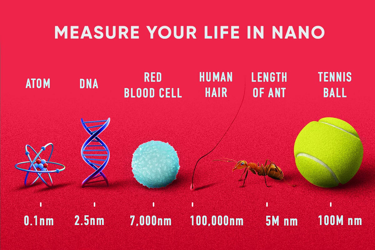
One nanometer is equal to one-billionth of a meter (0.000000001 m). In scientific notation, it is expressed as 10⁻⁹ meters. To visualize this microscopic scale, consider that a single sheet of paper is approximately 100,000 nanometers thick, and a human hair averages between 80,000 and 100,000 nanometers in diameter.
The Mathematical Definition of a Nanometer
To comprehend what 1 nanometer is equal to, one must first understand its position within the International System of Units (SI). The prefix "nano-" is derived from the Greek word nanos, meaning "dwarf." In the hierarchy of metric measurements, the nanometer (nm) sits three orders of magnitude below the micrometer (µm) and three orders of magnitude above the picometer (pm).
Mathematically, 1 nanometer is defined as:
- 0.001 micrometers (microns)
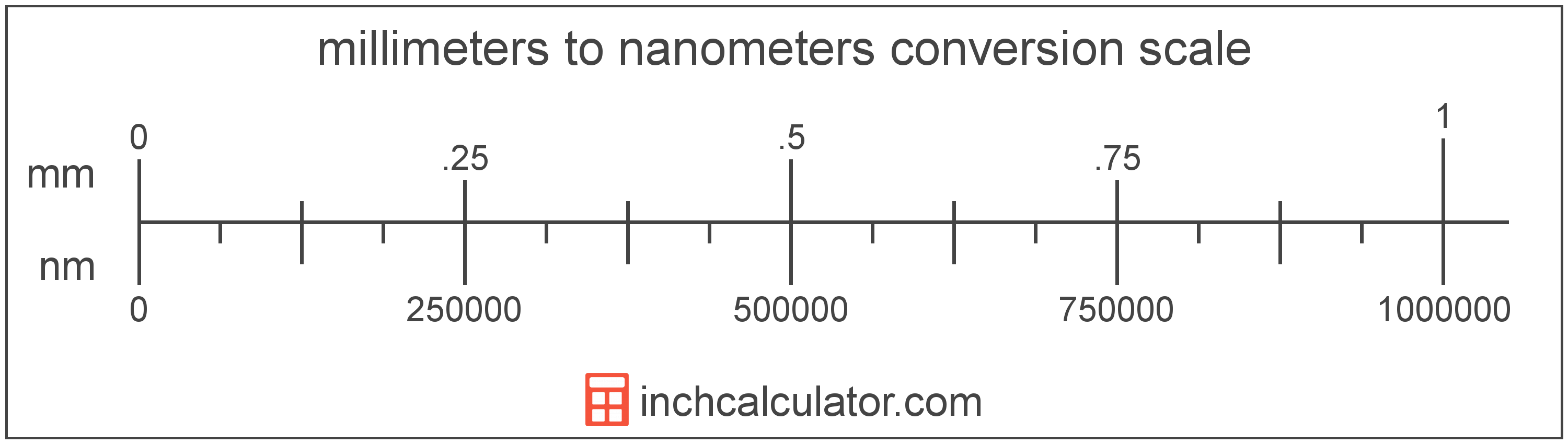
- 0.000001 millimeters
- 0.0000001 centimeters
- 0.000000001 meters
In terms of atomic scales, 1 nanometer is exactly equal to 10 Angstroms (Å). This is a critical conversion factor in physics and chemistry because the diameter of a single hydrogen atom is approximately 0.1 nanometers. Therefore, a line of ten hydrogen atoms placed side-by-side would measure roughly one nanometer in length. Understanding this relationship is essential for researchers working in molecular biology and solid-state physics, where measurements often fluctuate between the nanometer and Angstrom scales.
The precision of this measurement is maintained by the International Bureau of Weights and Measures (BIPM), which ensures that the meter—and by extension, the nanometer—is defined by the speed of light in a vacuum. As of 2026, the consistency of these sub-atomic measurements remains the bedrock of global scientific collaboration.
Converting 1 Nanometer to Imperial Units
While the scientific community almost exclusively uses the metric system, industrial applications in the United States often require conversions to imperial units. Because the nanometer is so small, these conversions result in extremely low decimal values that are typically managed using scientific notation.
One nanometer is approximately equal to 0.00000003937 inches. To put this in a more manageable perspective, there are exactly 25,400,000 nanometers in a single inch. This staggering ratio highlights why the imperial system is rarely used in nanotechnology or semiconductor fabrication; the numbers become too cumbersome for practical engineering.
In the context of machining and high-precision manufacturing, "mils" or "thous" (thousandths of an inch) are common. One nanometer is roughly 0.00003937 mils. When engineers in 2026 discuss "ultra-precision" tolerances, they are often bridging the gap between these two systems, requiring specialized software to ensure that conversion errors do not compromise the integrity of components designed at the nanoscale.
Visualizing the Nanoscale: Relatable Comparisons
Because the human eye cannot perceive anything smaller than approximately 10,000 to 40,000 nanometers (the width of a very fine fiber), we must rely on analogies to understand the scale of 1 nanometer.
If we were to expand a single nanometer to the length of a marble, then a meter would be the size of the Earth. This "Earth-to-marble" comparison is the standard pedagogical tool for illustrating the billion-to-one ratio inherent in the metric system. Another common visualization is the growth of a fingernail; on average, a human fingernail grows approximately one nanometer every second.
In the world of biology, the scale of 1 nanometer is the domain of molecules. A strand of human DNA is roughly 2.5 nanometers in diameter. A cell membrane is about 7 to 10 nanometers thick. When we speak of "nanotechnology," we are referring to the manipulation of matter at this specific level—where the properties of materials begin to change due to quantum effects. At 1 nanometer, the surface-area-to-volume ratio becomes so high that chemical reactivity increases dramatically, a principle that drives modern catalyst design and targeted drug delivery systems.
The Role of the Nanometer in Semiconductor Technology
As of 2026, the term "nanometer" is most frequently encountered in the marketing and technical specifications of computer processors. For decades, the semiconductor industry followed Moore's Law, shrinking the "process node" size to fit more transistors onto a silicon chip.
However, it is important to clarify a common misconception: the "2nm" or "1.4nm" (A14) labels used by companies like TSMC, Intel, and Samsung do not always refer to a specific physical dimension of a transistor gate. Instead, these names are commercial designations for a generation of technology that offers a certain density and power efficiency equivalent to what a theoretical 2nm or 1.4nm node would provide.
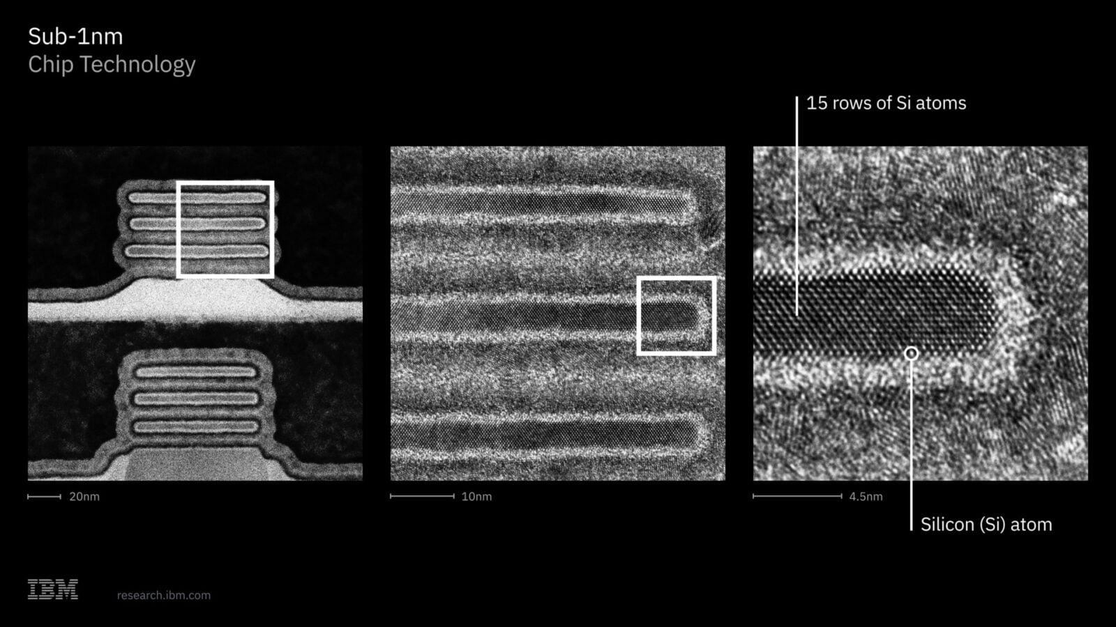
In 2026, we have transitioned into the "Angstrom Era," where manufacturers are discussing "A14" (1.4nm) and "A10" (1nm) nodes. At this level, the physical limits of silicon are being reached. When a transistor gate becomes as thin as 1 nanometer—roughly the width of five silicon atoms—electrons can "leak" through the barrier via a phenomenon called quantum tunneling. This has necessitated the move to new transistor architectures, such as Gate-All-Around (GAA) FETs and complementary FETs (CFETs), to maintain control over the electrical current at the one-nanometer scale.
Comparison of Measurements at the Nanoscale
The following table provides a comprehensive reference for how 1 nanometer relates to other common units of measurement used in science and industry.
| Unit Name | Symbol | Value in 1 Nanometer | Scientific Notation |
|---|---|---|---|
| Meter | m | 0.000000001 | 1 x 10⁻⁹ m |
| Centimeter | cm | 0.0000001 | 1 x 10⁻⁷ cm |
| Millimeter | mm | 0.000001 | 1 x 10⁻⁶ mm |
| Micrometer (Micron) | µm | 0.001 | 1 x 10⁻³ µm |
| Angstrom | Å | 10 | 10¹ Å |
| Picometer | pm | 1,000 | 1 x 10³ pm |
| Inch | in | 0.00000003937 | 3.937 x 10⁻⁸ in |
| Mil (Thou) | mil | 0.00003937 | 3.937 x 10⁻⁵ mil |
How Scientists Measure and Observe the Nanometer
Because 1 nanometer is significantly smaller than the wavelength of visible light (which ranges from 400 to 700 nanometers), it is impossible to see a nanometer using a traditional optical microscope. This limitation is known as the "diffraction limit." To observe objects at the 1nm scale, scientists must use specialized instruments that do not rely on light.
Electron Microscopy
Transmission Electron Microscopes (TEM) and Scanning Electron Microscopes (SEM) use beams of electrons instead of photons. Since electrons have much shorter wavelengths than light, they can resolve features down to a fraction of a nanometer. By 2026, advanced aberration-corrected TEMs allow researchers to visualize individual atoms within a crystal lattice, providing the visual proof needed to verify that a structure is indeed 1 nanometer wide.
Scanning Probe Microscopy
The Scanning Tunneling Microscope (STM) and the Atomic Force Microscope (AFM) take a different approach. Instead of using a beam, these tools use an ultra-fine physical probe that "feels" the surface of a sample. In an STM, an electrical current "tunnels" between the probe tip and the surface. By maintaining a constant current, the probe maps out the atomic topography of the surface. This technology was so revolutionary that its inventors were awarded the Nobel Prize in Physics in 1986, and it remains the gold standard for measuring 1 nanometer accurately in 2026.
Why 1 Nanometer Matters in 2026
The significance of the nanometer has shifted from a purely scientific curiosity to a cornerstone of the global economy. In 2026, the mastery of the 1-nanometer scale influences several key sectors:
- Medicine: "Nanobots" and lipid nanoparticles are designed at the 1-100nm scale to bypass the body’s immune system and deliver mRNA or chemotherapy directly to specific cells.
- Materials Science: Carbon nanotubes, which are often only 1-2 nanometers in diameter, are being integrated into structural materials to create composites that are significantly stronger than steel but a fraction of the weight.
- Environmental Science: Nanoporous membranes with pore sizes near 1 nanometer are used for high-efficiency desalination, allowing water molecules to pass through while blocking salt ions and contaminants.
- Quantum Computing: The qubits used in quantum processors rely on junctions and barriers measured at the nanometer scale. The precision of these 1nm layers determines the stability and "coherence" of the quantum state.
The National Nanotechnology Initiative (NNI) continues to oversee the federal coordination of research in this area, emphasizing that the 1nm to 100nm range is where the most significant technological breakthroughs are currently occurring.
FAQs About Nanometer Measurements
Can you see 1 nanometer with a magnifying glass?
No. A magnifying glass or a standard optical microscope is limited by the wavelength of visible light. The smallest feature a high-end optical microscope can resolve is about 200 nanometers. To see 1 nanometer, you require an electron microscope or a scanning probe microscope.
How many atoms fit into 1 nanometer?
It depends on the element, but as a rule of thumb, about 3 to 5 atoms can fit into a single nanometer. For example, a gold atom has a diameter of roughly 0.28 nanometers, so approximately 3.5 gold atoms lined up would equal 1 nanometer.
Is a virus 1 nanometer in size?
No, most viruses are much larger. A typical virus ranges from 20 to 300 nanometers. For instance, the influenza virus is roughly 80-120 nanometers in diameter. While a virus is "nanoscopic," it is still composed of thousands of molecules and is significantly larger than the 1-nanometer mark.
Why is the 1nm scale called the "Quantum Realm"?
At the 1-nanometer scale, the classical laws of physics (like those described by Newton) begin to break down, and quantum mechanical effects become dominant. At this size, electrons behave more like waves than particles, and properties like electrical conductivity and color can change based on the size of the particle rather than its material composition.
Is 1 nanometer safe for human exposure?
The safety of nanometer-scale particles (nanoparticles) depends entirely on their chemical composition and shape. Because 1-nanometer particles are small enough to enter human cells and even the nucleus, researchers in 2026 follow strict "nanotoxicology" protocols to ensure that engineered nanomaterials do not pose a health risk.
Practical Recommendation for Working with Nanometers
When calculating or documenting measurements at the 1-nanometer scale, it is highly recommended to use scientific notation (10⁻⁹ m) rather than decimal points to avoid catastrophic rounding errors. In professional engineering and laboratory settings, always verify the "calibration state" of your AFM or SEM against a certified standard, such as those provided by the National Institute of Standards and Technology (NIST). As we push further into the Angstrom era in 2026, the margin for error is effectively zero; a mistake of even 0.5 nanometers can lead to the failure of a semiconductor node or a chemical reaction.