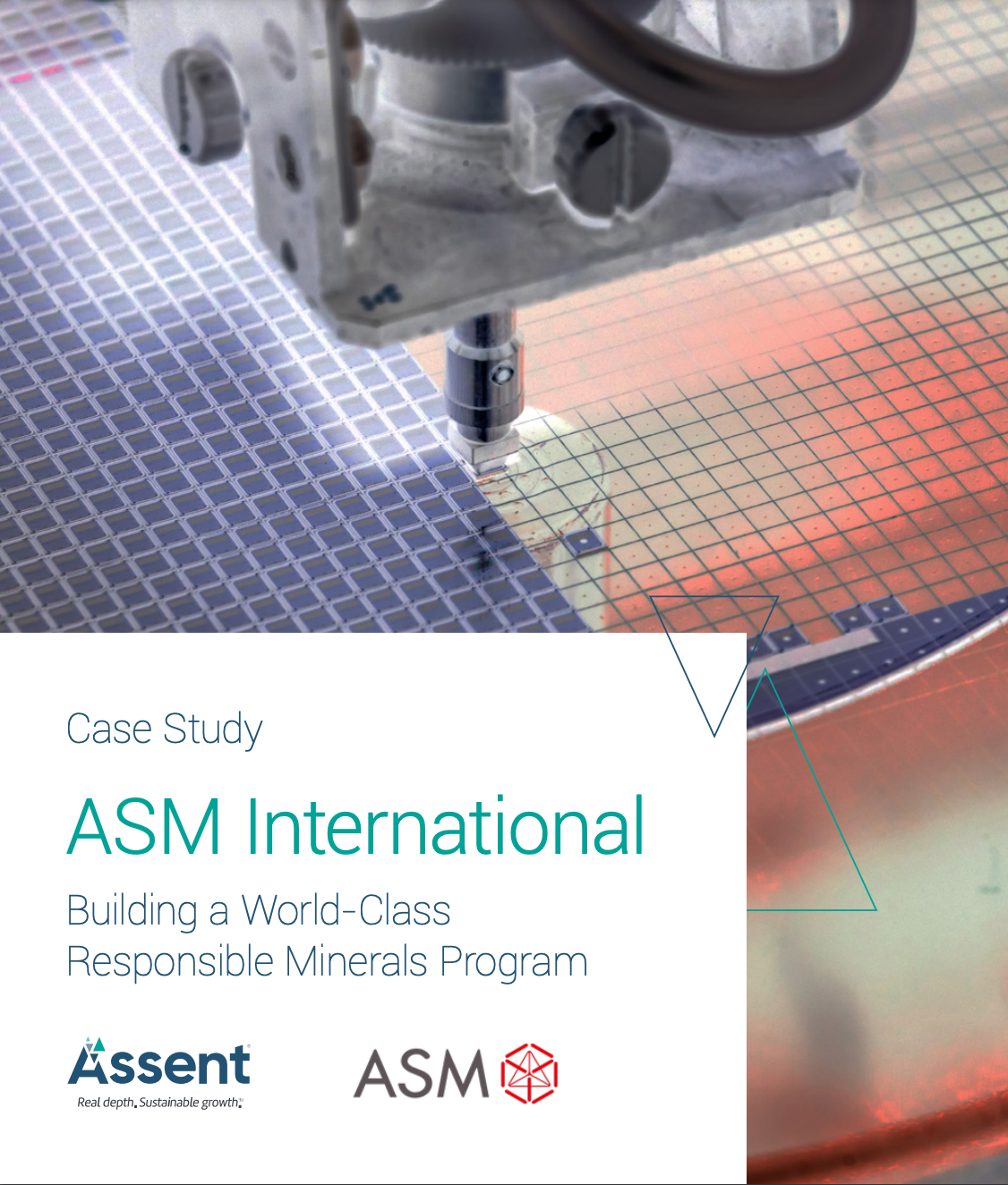
ASM International stands as a pivotal force in the global semiconductor manufacturing ecosystem and materials engineering sector, known for pioneering advanced deposition technologies such as Atomic Layer Deposition (ALD) and Epitaxy. The company operates at the leading edge of microelectronics fabrication, providing the critical equipment and processes required by top-tier chipmakers to build increasingly smaller, faster, and more energy-efficient integrated circuits.
Understanding ASM International: Corporate Overview and Market Position
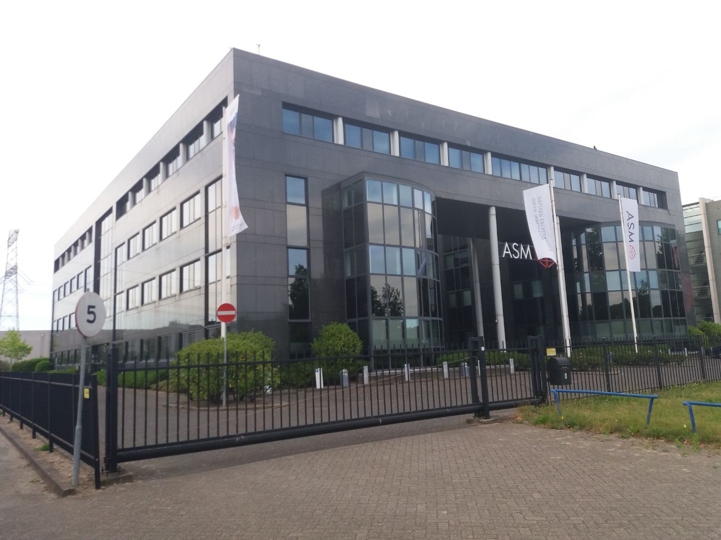
ASM International N.V. is a specialized global supplier of semiconductor process equipment, focusing on wafer processing solutions for front-end semiconductor manufacturing. Headquartered in Almere, Netherlands, the company holds a distinct position in the global supply chain, maintaining research, manufacturing, and support operations across Europe, Asia, and the United States.
The primary search intent for "ASM International" typically bridges two distinct domains: potential investors looking at financial performance and market capitalization, and engineering professionals or researchers seeking technical details on semiconductor fabrication equipment. To resolve this ambiguity, this guide focuses primarily on its identity as a global semiconductor equipment manufacturer, detailing its core technological contributions, operational landscape, and industry significance.
Corporate Structure and Global Footprint
Unlike massive turnkey semiconductor equipment conglomerates that cover every aspect of wafer fabrication, ASM International maintains a targeted focus on deposition technologies. Its operational model relies heavily on close collaboration with leading logic, foundry, and memory manufacturers. By co-locating research and development teams near major semiconductor hubs in countries like South Korea, Taiwan, Japan, the United States, and Singapore, the organization ensures rapid feedback loops and customized equipment optimization for shrinking technology nodes.
Historical Evolution
Founded in 1968, ASM (Advanced Semiconductor Materials) has evolved from a local supplier of assembly and packaging equipment into a tier-one front-end wafer processing equipment provider. Over the decades, the company divested various non-core segments—most notably spinning off its assembly and packaging business into ASMPT—while aggressively channeling capital into thin-film deposition R&D. This strategic shift positioned ASM as an early pioneer and eventual market leader in Atomic Layer Deposition, a technology that became indispensable as semiconductor features shrank to the nanoscale.
Core Technologies: ALD and Epitaxy Leadership
At the heart of ASM International’s industry standing are its proprietary deposition technologies. Deposition is the process of adding extremely thin layers of atoms or molecules onto a silicon wafer. As microprocessors and memory cells transition into three-dimensional architectures (such as FinFETs, Gate-All-Around nanosheets, and advanced 3D NAND flash), traditional deposition methods fail to coat complex surfaces evenly. ASM addresses this challenge through advanced chemical solutions.
Atomic Layer Deposition (ALD)
Atomic Layer Deposition is a self-limiting, sequential surface chemistry technique that deposits films one atomic layer at a time. ASM is widely recognized as a pioneer of commercial high-volume manufacturing ALD tools.
- Conformal Coating: ALD provides absolute uniformity and conformity on ultra-high aspect ratio structures, coating the sidewalls and bottoms of deep trenches without pinching off the opening.
- High-k Dielectrics: ALD enabled the transition from silicon dioxide to high-k metal gate stacks, preventing quantum leakage currents in advanced transistors.
- Spacer Lithography: Semiconductor manufacturing relies heavily on self-aligned multi-patterning techniques enabled by precise spacer deposition via low-temperature ALD.
Epitaxy
Epitaxy involves growing a crystalline layer on a crystalline substrate, matching the orientation of the underlying crystal lattice. ASM provides advanced single-wafer epitaxial reactors used for strained silicon, source/drain engineering, and advanced channel materials in advanced logic nodes. These systems require precise thermal management and rapid gas-switching capabilities to ensure abrupt chemical interfaces and optimal electrical carrier mobility.
Product Portfolio and Wafer Processing Solutions
ASM International's product lineup is engineered to address specific process modules within the semiconductor fabrication sequence. The portfolio centers primarily on single-wafer reactors designed for high throughput, exceptional wafer-to-wafer repeatability, and minimal particle generation.
| Product Family | Primary Technology | Core Applications | Key Operational Advantages |
|---|---|---|---|
| Intrepid | Epitaxy | Silicon-germanium (SiGe) source/drain, channel growth | Superior thermal uniformity, precise profile control |
| Pulsion | Atomic Layer Deposition | High-k gate dielectrics, metal gates, DRAM capacitors | High throughput, precise thickness control at atomic scale |
| EmerALD | Atomic Layer Deposition | Advanced interconnects, barrier layers, advanced logic | Low thermal budget, excellent step coverage on 3D structures |
| A400 / Pulsar | Batch and Single-Wafer ALD/CVD | Legacy and mainstream semiconductor nodes | Proven reliability, high uptime, cost-effective manufacturing |
The Semiconductor Equipment Ecosystem and Supply Chain Dynamics
Operating within the semiconductor industry requires navigating complex global supply chains, stringent purity standards, and cyclical market demands. ASM International operates in a highly concentrated competitive landscape alongside giants such as Applied Materials, Lam Research, and Tokyo Electron.
R&D Intensity and Customer Collaboration
The semiconductor equipment sector is characterized by immense research and development expenditures. Chipmakers establish technology roadmaps years in advance, requiring equipment suppliers like ASM to co-develop tools before commercial production runs begin. This process, known as joint development programs (JDPs), ensures that ASM's deposition chambers are tailored to the exact physical and chemical parameters required for upcoming node transitions, such as sub-2nm gate-all-around architectures.
Cyclicality and Market Exposure
Like its peers, ASM is subject to the cyclical nature of the global semiconductor market. Demand swings are driven by end-market consumption in smartphones, personal computers, automotive electronics, and artificial intelligence infrastructure. To mitigate downturns, the company maintains a diversified customer base spanning major logic foundries, memory makers, and specialty chip manufacturers.
Environmental, Social, and Governance (ESG) Considerations in Wafer Fabrication
Modern semiconductor manufacturing places heavy emphasis on sustainability, energy efficiency, and chemical safety. Equipment manufacturers face intense pressure to reduce the environmental footprint of their tools while operating inside ultra-clean environments (cleanrooms).
- Energy and Chemical Efficiency: Advanced deposition tools are engineered to optimize precursor gas utilization, minimizing expensive chemical waste and reducing greenhouse gas emissions associated with plasma generation and thermal processing.
- Greenhouse Gas Reduction: ASM has aligned its corporate strategy with science-based targets to reduce Scope 1, Scope 2, and Scope 3 carbon emissions, targeting carbon neutrality across its direct operations and supply chain.
- Safety Protocols: Handling hazardous precursor chemicals requires rigorous fail-safe systems, automated gas delivery modules, and continuous exhaust monitoring to protect facility personnel.
Frequently Asked Questions
What is ASM International best known for in the semiconductor industry?
ASM International is best known for pioneering and supplying advanced Atomic Layer Deposition (ALD) and epitaxy equipment. These tools are critical for depositing ultra-thin, highly uniform atomic layers required to manufacture modern logic chips, memory devices, and 3D transistors.
Where is ASM International headquartered?
ASM International is headquartered in Almere, Netherlands. However, it operates a global network of research, development, manufacturing, and customer support facilities across Europe, Asia, and North America to serve local semiconductor fabrication plants.
What is the difference between ASM International and ASMPT?
While they share historical roots, ASM International focuses strictly on front-end wafer processing equipment (such as deposition and epitaxy tools). ASMPT (ASM Pacific Technology), in which ASM International holds a major stake, specializes in back-end semiconductor manufacturing equipment, including assembly, packaging, and surface mount technology solutions.
How does Atomic Layer Deposition (ALD) work in semiconductor manufacturing?
ALD is a chemical vapor deposition process that uses sequential, self-limiting surface reactions. Precursor gases are pulsed into a reaction chamber one at a time, separated by inert gas purges. This ensures that exactly one atomic layer is deposited per cycle, yielding exceptional thickness control and conformal coverage on complex 3D structures.
Why are deposition tools crucial for sub-2nm semiconductor nodes?
As semiconductor features shrink below 2nm, traditional deposition methods cannot coat the vertical sidewalls of advanced transistor architectures evenly. Deposition tools like ASM’s ALD systems provide precise, atomic-level control necessary to prevent electrical leakage, reduce resistance, and maintain structural integrity in next-generation microchips.
Conclusion and Strategic Outlook
ASM International occupies a vital niche in the global microelectronics supply chain. By maintaining an unyielding focus on thin-film deposition technologies—specifically Atomic Layer Deposition and advanced epitaxy—the company has secured an indispensable role in enabling Moore’s Law and the transition to advanced 3D chip architectures. For semiconductor engineers, understanding ASM's tool capabilities is essential for process optimization; for industry observers, the company remains a primary barometer for technological health and capital expenditure trends at the leading edge of semiconductor manufacturing.