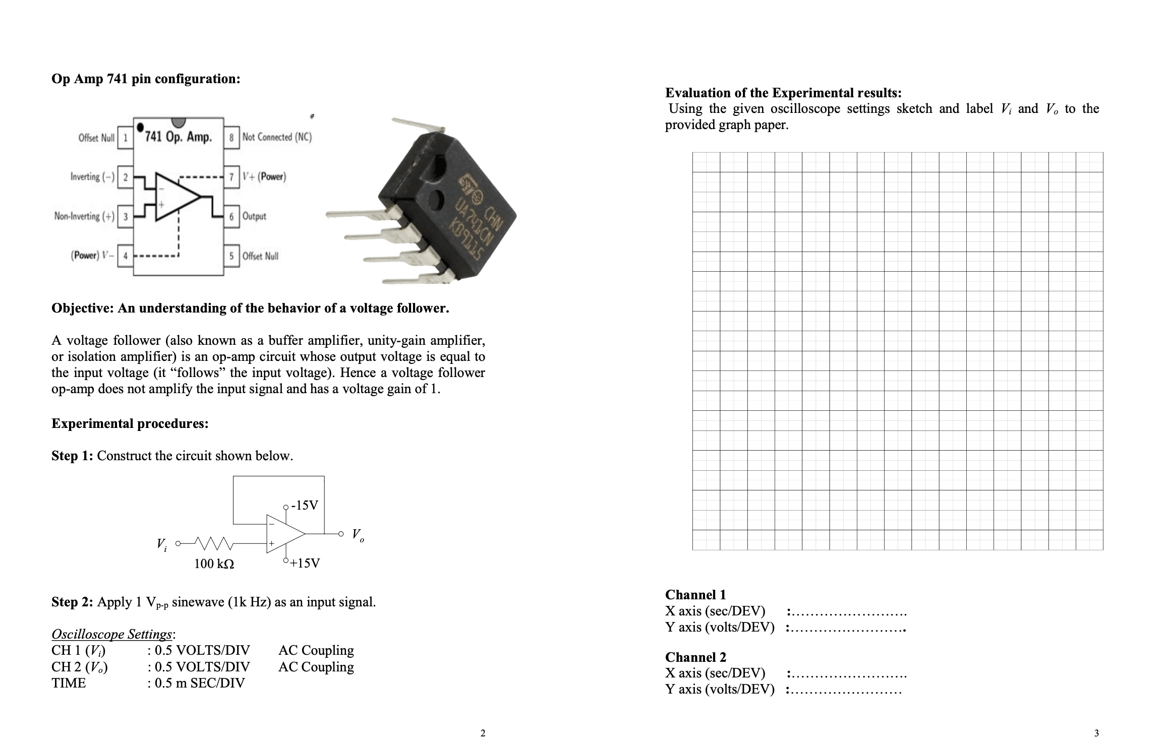
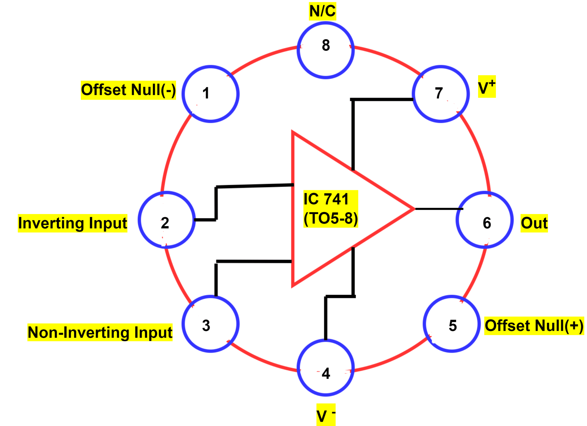
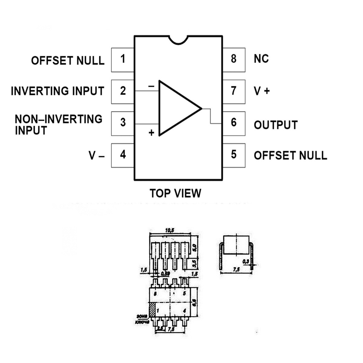
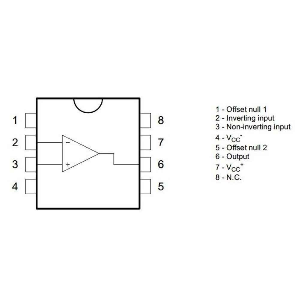
The 741 operational amplifier pin configuration consists of an 8-pin layout, typically in a Dual In-line Package (DIP). It features two input pins (inverting and non-inverting), two power supply pins (V+ and V-), one output pin, and two offset null pins used for fine-tuning, alongside one "no connection" pin.
The LM741 operational amplifier (op-amp) remains one of the most iconic and enduring integrated circuits in the history of electronics. First introduced by Fairchild Semiconductor in the late 1960s, it set the standard for internally compensated op-amps. As of 2026, while modern CMOS and high-speed BiFET op-amps have surpassed it in performance, the 741 remains a fundamental component for education, basic signal conditioning, and low-frequency analog circuits. Understanding its pin configuration is the first step for any engineer or student looking to master analog circuit design.
Understanding the 8-Pin DIP Layout
The most common physical form of the 741 op-amp is the 8-pin plastic Dual In-line Package (DIP). To correctly identify the pins, you must orient the IC so that the semi-circular notch or dot at one end faces upward or to the left. When the notch is at the top, Pin 1 is the top-left pin, and the numbers proceed counter-clockwise down to Pin 4 and then up from Pin 5 to Pin 8.
The 741 is also available in metal can packages (TO-5) and surface-mount (SOIC) packages, but the 8-pin DIP is the standard for breadboarding and prototyping. Each pin serves a specific role in the internal circuitry, facilitating the high-gain differential amplification that the device is known for.
Detailed Breakdown of the 741 Pin Functions
Each of the eight pins on the 741 op-amp is critical to its operation. Understanding the electrical characteristics and purpose of these pins allows for more robust circuit design and easier troubleshooting.
Pin 1 and Pin 5: Offset Null
The 741 is a bipolar integrated circuit. Due to slight manufacturing variations in the internal transistors, the output voltage may not be exactly zero when both input pins are at the same voltage. This is known as "input offset voltage." Pins 1 and 5 are provided to "null" or cancel out this offset.
To use these pins, a potentiometer (typically 10kΩ) is connected between Pin 1 and Pin 5, with the potentiometer's wiper connected to the negative power supply (Pin 4). By adjusting the wiper, the user can balance the internal currents and force the output to zero when the inputs are grounded. In most general-purpose applications, these pins are left unconnected.
Pin 2: Inverting Input (-)
The inverting input is one half of the differential input pair. When a signal is applied to this pin while the non-inverting input is held at a constant voltage, the output will be 180 degrees out of phase with the input. If the input voltage at Pin 2 increases, the output voltage at Pin 6 decreases. This pin is central to feedback loops in inverting amplifier configurations.
Pin 3: Non-Inverting Input (+)
The non-inverting input is the second half of the differential pair. A signal applied here produces an output that is in phase with the input. If the voltage at Pin 3 increases, the output voltage at Pin 6 also increases. In many sensor applications, the signal is fed into Pin 3 to maintain the original polarity of the data.
Pin 4: V- (Negative Power Supply)
The 741 is designed to operate primarily on a dual or bipolar power supply. Pin 4 is connected to the negative rail. While modern op-amps are often "rail-to-rail," the 741 requires a significant voltage margin. For a standard ±15V setup, Pin 4 is connected to -15V. It is important to note that if you are using a single-ended power supply, Pin 4 is connected to ground, but the circuit must be biased to a "virtual ground" to function correctly.
Pin 6: Output
Pin 6 provides the amplified signal. The output of the 741 is protected against short circuits, meaning it can withstand a direct connection to ground or either power rail for a short duration without immediate destruction. However, the output voltage swing is limited; it generally cannot reach the full supply voltage. Usually, the output stays within 1.5 to 2 volts of the V+ and V- rails.
Pin 7: V+ (Positive Power Supply)
This pin connects to the positive terminal of the power supply. The maximum supply voltage for a standard LM741 is typically ±18V, though most applications utilize ±12V or ±15V. Proper decoupling using a 0.1µF ceramic capacitor placed close to Pin 7 and Pin 4 is recommended to prevent high-frequency oscillations.
Pin 8: NC (No Connection)
Pin 8 is not connected to any internal circuitry within the 741 IC. It exists primarily to complete the standard 8-pin DIP package symmetry. In PCB layout, this pin is often left floating, or used as a convenient "anchor" point for traces that do not interact with the op-amp logic.
Key Technical Specifications of the 741
To design effectively with the 741 pin configuration, one must understand the electrical limits and performance metrics. The following table outlines the standard characteristics for the LM741 as recognized in current 2026 engineering documentation.
| Parameter | Typical Value | Absolute Maximum |
|---|---|---|
| Supply Voltage ($V_{CC}$) | ±15V | ±18V to ±22V (model dependent) |
| Power Dissipation | 500 mW | 670 mW |
| Differential Input Voltage | ±30V | ±30V |
| Input Offset Voltage | 1.0 mV to 5.0 mV | 6.0 mV |
| Slew Rate | 0.5 V/µs | N/A |
| Bandwidth (Unity Gain) | 1.0 MHz | N/A |
| Input Resistance | 2 MΩ | N/A |
| Output Short Circuit Duration | Continuous | Continuous |
Power Supply Considerations and Pin Interaction
The 741 is notoriously picky about its power supply. Unlike some modern "single-supply" op-amps, the 741's internal architecture is optimized for symmetric power.
Dual Supply Mode
In a dual supply mode, Pin 7 might be at +15V and Pin 4 at -15V. This allows the output (Pin 6) to swing both positive and negative relative to the common ground. This is essential for AC signal processing, such as audio amplification, where the waveform must cross the zero-volt axis.
Single Supply Mode
To use the 741 with a single supply (e.g., Pin 7 at +12V and Pin 4 at Ground), you must create a virtual ground. This involves using a voltage divider to set the non-inverting input (Pin 3) to half the supply voltage (6V). The output will then oscillate around this 6V midpoint. This configuration is common in battery-operated devices but reduces the available "headroom" for the signal.
Common Circuit Configurations Using the 741 Pinout
The versatility of the 741's 8-pin configuration allows it to be wired into several "classic" circuits. Each configuration utilizes the pins in a specific way to define the relationship between input and output.
1. The Inverting Amplifier
In this setup, the non-inverting input (Pin 3) is connected to ground. The input signal is fed through a resistor to the inverting input (Pin 2). A feedback resistor is connected between the output (Pin 6) and the inverting input (Pin 2). The gain is determined by the ratio of these two resistors. Because Pin 2 is an inverting input, the output is the inverted version of the input signal.
2. The Non-Inverting Amplifier
Here, the input signal is applied directly to Pin 3. The feedback network (two resistors) is connected to Pin 2 and ground. This configuration provides a high input impedance, which is ideal for measuring signals from high-resistance sensors without "loading" the source. The output at Pin 6 stays in phase with the input at Pin 3.
3. The Voltage Follower (Buffer)
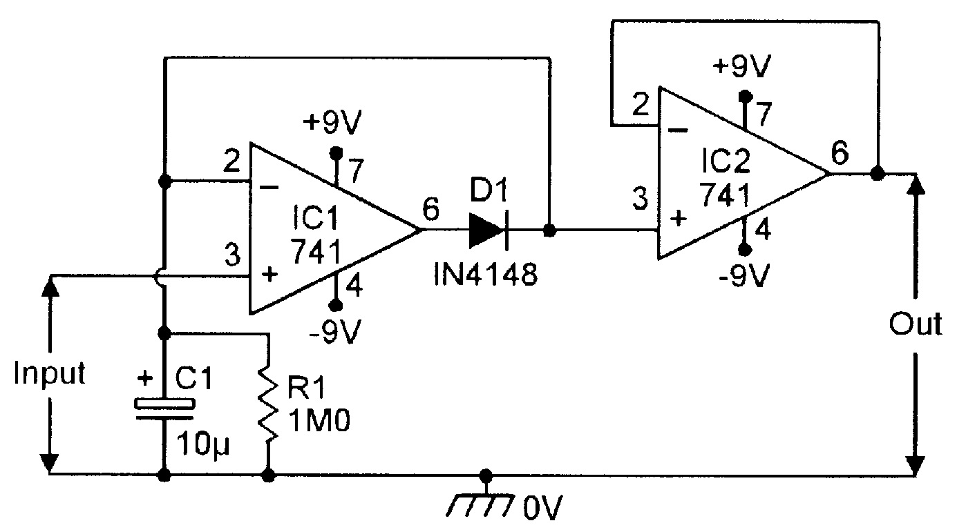
This is the simplest configuration. The output (Pin 6) is connected directly back to the inverting input (Pin 2), and the signal is fed into the non-inverting input (Pin 3). The gain is exactly 1. This uses the 741's high input impedance and low output impedance to isolate different stages of a circuit, preventing one stage from affecting the performance of the next.
Limitations and Practical Advice for 2026
While the 741 is a "workhorse," its 8-pin configuration hides several performance bottlenecks that modern designers must account for.
- Slew Rate: The 741 has a slow slew rate of approximately 0.5V/µs. This means it cannot respond quickly to fast-changing signals. If you try to amplify a high-frequency square wave, the 741 output will look like a triangle wave because it cannot "keep up" with the sharp edges.
- Noise and Precision: For high-fidelity audio or precision medical instrumentation, the 741 is generally too noisy. Modern alternatives like the OPA2134 or the TL071 (which shares a similar pinout) offer much better performance.
- Voltage Rails: Always remember that the 741 is not a rail-to-rail op-amp. If you power it with 5V, your output might only be able to swing between 1.5V and 3.5V. This makes it a poor choice for modern 3.3V digital systems.
Troubleshooting the 741 Pin Configuration
If your 741 circuit is not behaving as expected, check the following common issues:
- Pin Orientation: Ensure the IC is not backwards. Pin 1 must align with the notch.
- Floating Inputs: Never leave an input pin (2 or 3) disconnected. Even if you aren't using one, it should be tied to ground or a reference voltage. A floating input will pick up electromagnetic interference and cause the output to saturate at one of the power rails.
- Power Supply Decoupling: If the output is oscillating or showing random noise, place a 0.1µF capacitor between Pin 7 and Ground, and another between Pin 4 and Ground.
- Common Mode Range: Ensure the voltage at the input pins (2 and 3) is at least 2-3 volts away from the power supply rails. If the inputs get too close to V+ or V-, the internal transistors may saturate, a condition sometimes called "latch-up."
FAQs About 741 Op Amp Pinout
Can I use the 741 with a single 9V battery?
Yes, you can use a single 9V battery by connecting the positive terminal to Pin 7 and the negative terminal to Pin 4. However, you must bias the inputs to approximately 4.5V (using a voltage divider) so the signal has room to swing up and down. Without this bias, the 741 will not amplify AC signals correctly.
Why does the 741 have an NC pin?
The NC (No Connection) at Pin 8 is primarily for mechanical stability and standardizing the package size. Most low-power integrated circuits utilize the 8-pin DIP format. By keeping Pin 8 as a dummy pin, manufacturers can use the same lead frames and assembly machines used for other 8-pin ICs.
Is the 741 pinout the same as the TL071 or LM358?
The 741 pinout is identical to the TL071 (a JFET-input op-amp), making them "drop-in" replacements for one another. However, it is not the same as the LM358. The LM358 is a dual op-amp in an 8-pin package, meaning it contains two separate amplifiers with a completely different pin mapping.
What happens if I swap Pin 4 and Pin 7?
Swapping the power supply pins (applying positive voltage to Pin 4 and negative to Pin 7) will likely destroy the internal transistors of the 741 almost instantly. Most versions of the 741 do not have reverse-polarity protection.
Do I need to connect Pins 1 and 5 for the circuit to work?
No, for the vast majority of hobbyist and educational projects, Pins 1 and 5 (Offset Null) should be left completely disconnected. The natural offset of the 741 is usually small enough that it won't affect basic LED drivers, oscillators, or simple amplifiers.
Final Recommendations
When working with the 741 op amp pin configuration, always start by verifying your power supply rails with a multimeter before inserting the IC into your breadboard. For those learning electronics in 2026, the 741 remains the best vehicle for understanding the "Golden Rules" of op-amps due to its forgiving nature and well-documented behavior. If your project requires high speed or battery efficiency, consider using the 741 pinout as a template to eventually migrate to more modern chips like the TL071 or the OP07 for higher precision.